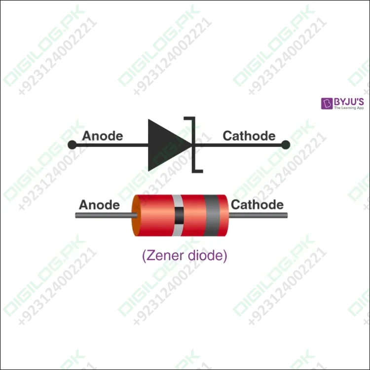
Zener Diode In Pakistan
A Zener diode is a special type of diode designed to reliably allow current to flow "backwards" (inverted polarity) when a certain set reverse voltage, known as the Zener voltage, is reached.
Zener diodes are manufactured with a great variety of Zener voltages and some are even variable. Some Zener diodes have an abrupt, heavily doped p–n junction with a low Zener voltage, in which case the reverse conduction occurs due to electron quantum tunnelling in the short distance between p and n regions − this is known as the Zener effect, after Clarence Zener. Diodes with a higher Zener voltage have lighter doped junctions which causes their mode of operation to involve avalanche breakdown. Both breakdown types are present in Zener diodes with the Zener effect predominating at lower voltages and avalanche breakdown at higher voltages.
They are used to generate low-power stabilized supply rails from a higher voltage and to provide reference voltages for circuits, especially stabilized power supplies. They are also used to protect circuits from overvoltage, especially electrostatic discharge.
History
[edit]The device is named after American physicist Clarence Zener who first described the Zener effect in 1934 in his primarily theoretical studies of breakdown of electrical insulator properties. Later, his work led to the Bell Labs implementation of the effect in form of an electronic device, the Zener diode.[1]
Operation
[edit]A conventional solid-state diode allows significant current if it is reverse-biased above its reverse breakdown voltage. When the reverse bias breakdown voltage is exceeded, a conventional diode will conduct a high current due to avalanche breakdown. Unless this current is limited by external circuits, the diode may be permanently damaged due to overheating at the small (localized) areas of the semiconductor junction where avalanche breakdown conduction is occurring. A Zener diode exhibits almost the same properties, except the device is specially designed so as to have a reduced breakdown voltage, the so-called Zener voltage. By contrast with the conventional device, a reverse-biased Zener diode exhibits a controlled breakdown and allows the current to keep the voltage across the Zener diode close to the Zener breakdown voltage. For example, a diode with a Zener breakdown voltage of 3.2 V exhibits a voltage drop of very nearly 3.2 V across a wide range of reverse currents. The Zener diode is therefore well suited for applications such as the generation of a reference voltage (e.g. for an amplifier stage), or as a voltage stabilizer for low-current applications.[2]
Another mechanism that produces a similar effect is the avalanche effect as in the avalanche diode.[2] The two types of diode are in fact constructed in a similar way and both effects are present in diodes of this type. In silicon diodes up to about 5.6 volts, the Zener effect is the predominant effect and shows a marked negative temperature coefficient. Above 5.6 volts, the avalanche effect dominates and exhibits a positive temperature coefficient.[3]
In a 5.6 V diode, the two effects occur together, and their temperature coefficients nearly cancel each other out, thus the 5.6 V diode is useful in temperature-critical applications. An alternative, which is used for voltage references that need to be highly stable over long periods of time, is to use a Zener diode with a temperature coefficient (TC) of +2 mV/°C (breakdown voltage 6.2–6.3 V) connected in series with a forward-biased silicon diode (or a transistor B-E junction) manufactured on the same chip.[4] The forward-biased diode has a temperature coefficient of −2 mV/°C, causing the TCs to cancel out for a net nearly zero temperature coefficient.
It is also worth noting that the temperature coefficient of a 4.7 V Zener diode is close to that of the emitter-base junction of a silicon transistor at around -2 mV/°C, so in a simple regulating circuit where the 4.7 V diode sets the voltage at the base of an NPN transistor (i.e. their coefficients are acting in parallel), the emitter will be at around 4 V and quite stable with temperature.
Modern designs have produced devices with voltages lower than 5.6 V with negligible temperature coefficients,[citation needed]. Higher voltage devices have a temperature coefficient that is approximately proportional to the amount by which the breakdown voltage exceeds 5 V. Thus a 75 V diode has 10 times the coefficient of a 12 V diode.[citation needed]
Zener and avalanche diodes, regardless of breakdown voltage, are usually marketed under the umbrella term of "Zener diode".
Under 5.6 V, where the Zener effect dominates, the IV curve near breakdown is much more rounded, which calls for more care in choosing its biasing conditions. The IV curve for Zeners above 5.6 V (being dominated by avalanche), is much more precise at breakdown.
Construction
[edit]The Zener diode's operation depends on the heavy doping of its p–n junction. The depletion region formed in the diode is very thin (<1 μm) and the electric field is consequently very high (about 500 kV/m) even for a small reverse bias voltage of about 5 V, allowing electrons to tunnel from the valence band of the p-type material to the conduction band of the n-type material.
At the atomic scale, this tunneling corresponds to the transport of valence band electrons into the empty conduction band states; as a result of the reduced barrier between these bands and high electric fields that are induced due to the high levels of doping on both sides.[3] The breakdown voltage can be controlled quite accurately by the doping process. Adding impurities, or doping, changes the behaviour of the semiconductor material in the diode. In the case of Zener diodes, this heavy doping creates a situation where the diode can operate in the breakdown region. While tolerances within 0.07% are available, commonly available tolerances are 5% and 10%. Breakdown voltage for commonly available Zener diodes can vary from 1.2 V to 200 V.
For diodes that are lightly doped, the breakdown is dominated by the avalanche effect rather than the Zener effect. Consequently, the breakdown voltage is higher (over 5.6 V) for these devices.[5]
Surface Zeners
[edit]The emitter-base junction of a bipolar NPN transistor behaves as a Zener diode, with breakdown voltage at about 6.8 V for common bipolar processes and about 10 V for lightly doped base regions in BiCMOS processes. Older processes with poor control of doping characteristics had the variation of Zener voltage up to ±1 V, newer processes using ion implantation can achieve no more than ±0.25 V. The NPN transistor structure can be employed as a surface Zener diode, with collector and emitter connected together as its cathode and base region as anode. In this approach the base doping profile usually narrows towards the surface, creating a region with intensified electric field where the avalanche breakdown occurs. Hot carriers produced by acceleration in the intense field can inject into the oxide layer above the junction and become trapped there. The accumulation of trapped charges can then cause 'Zener walkout', a corresponding change of the Zener voltage of the junction. The same effect can be achieved by radiation damage.
The emitter-base Zener diodes can handle only low currents as the energy is dissipated in the base depletion region which is very small. Higher amounts of dissipated energy (higher current for longer time, or a short very high current spike) causes thermal damage to the junction and/or its contacts. Partial damage of the junction can shift its Zener voltage. Total destruction of the Zener junction by overheating it and causing migration of metallization across the junction ("spiking") can be used intentionally as a 'Zener zap' antifuse.[6]
Subsurface Zeners
[edit]A subsurface Zener diode, also called 'buried Zener', is a device similar to the surface Zener, but the doping and design is such that the avalanche region is located deeper in the structure, typically several micrometers below the oxide. Hot carriers then lose energy by collisions with the semiconductor lattice before reaching the oxide layer and cannot be trapped there. The Zener walkout phenomenon therefore does not occur here, and the buried Zeners have stable voltage over their entire lifetime. Most buried Zeners have breakdown voltage of 5–7 volts. Several different junction structures are used.[7]
Uses
[edit]Zener diodes are widely used as voltage references and as shunt regulators to regulate the voltage across small circuits. When connected in parallel with a variable voltage source so that it is reverse biased, a Zener diode conducts when the voltage reaches the diode's reverse breakdown voltage. From that point on, the low impedance of the diode keeps the voltage across the diode at that value.[8]
In this circuit, a typical voltage reference or regulator, an input voltage, Uin (with + on the top), is regulated down to a stable output voltage Uout. The breakdown voltage of diode D is stable over a wide current range and holds Uout approximately constant even though the input voltage may fluctuate over a wide range. Because of the low impedance of the diode when operated like this, resistor R is used to limit current through the circuit.
In the case of this simple reference, the current flowing in the diode is determined using Ohm's law and the known voltage drop across the resistor R;
The value of R must satisfy two conditions:
- R must be small enough that the current through D keeps D in reverse breakdown. The value of this current is given in the data sheet for D. For example, the common BZX79C5V6[9] device, a 5.6 V 0.5 W Zener diode, has a recommended reverse current of 5 mA. If insufficient current exists through D, then Uout is unregulated and less than the nominal breakdown voltage (this differs from voltage-regulator tubes where the output voltage is higher than nominal and could rise as high as Uin). When calculating R, allowance must be made for any current through the external load, not shown in this diagram, connected across Uout.
- R must be large enough that the current through D does not destroy the device. If the current through D is ID, its breakdown voltage VB and its maximum power dissipation Pmax correlate as such: .
A load may be placed across the diode in this reference circuit, and as long as the Zener stays in reverse breakdown, the diode provides a stable voltage source to the load. Zener diodes in this configuration are often used as stable references for more advanced voltage regulator circuits.
Shunt regulators are simple, but the requirements that the ballast resistor be small enough to avoid excessive voltage drop during worst-case operation (low input voltage concurrent with high load current) tends to leave a lot of current flowing in the diode much of the time, making for a fairly wasteful regulator with high quiescent power dissipation, suitable only for smaller loads.
These devices are also encountered, typically in series with a base-emitter junction, in transistor stages where selective choice of a device centered on the avalanche or Zener point can be used to introduce compensating temperature co-efficient balancing of the transistor p–n junction. An example of this kind of use would be a DC error amplifier used in a regulated power supply circuit feedback loop system.
Zener diodes are also used in surge protectors to limit transient voltage spikes.
Noise generator
[edit]Another application of the Zener diode is using its avalanche breakdown noise (see noise generator § Zener diode), which for instance can be used for dithering in an analog-to-digital converter when at a rms level equivalent to 1⁄3 to 1 lsb[10] or to create a random number generator.
Waveform clipper
[edit]Two Zener diodes facing each other in series clip both halves of an input signal. Waveform clippers can be used not only to reshape a signal, but also to prevent voltage spikes from affecting circuits that are connected to the power supply.[11]
Voltage shifter
[edit]A Zener diode can be applied to a circuit with a resistor to act as a voltage shifter. This circuit lowers the output voltage by a quantity that is equal to the Zener diode's breakdown voltage.
Voltage regulator
[edit]A Zener diode can be applied in a voltage regulator circuit to regulate the voltage applied to a load, such as in a linear regulator.
See also
[edit]Voltage |
3.3V |
---|
-
aaaa, inv ok, si
📦 Free Shipping For 5000 Rupees Order
Enjoy free shipping across Pakistan. Terms & Conditions apply.
🛠️ Customer Support
Our support team is available Monday to Saturday, from 11:00 AM to 7:00 PM.
Phone: +92 312 4002221
Email: info@digilog.pk
💳 Payment Methods
- Bank Transfer: View Details
- Cash on Delivery By TCS