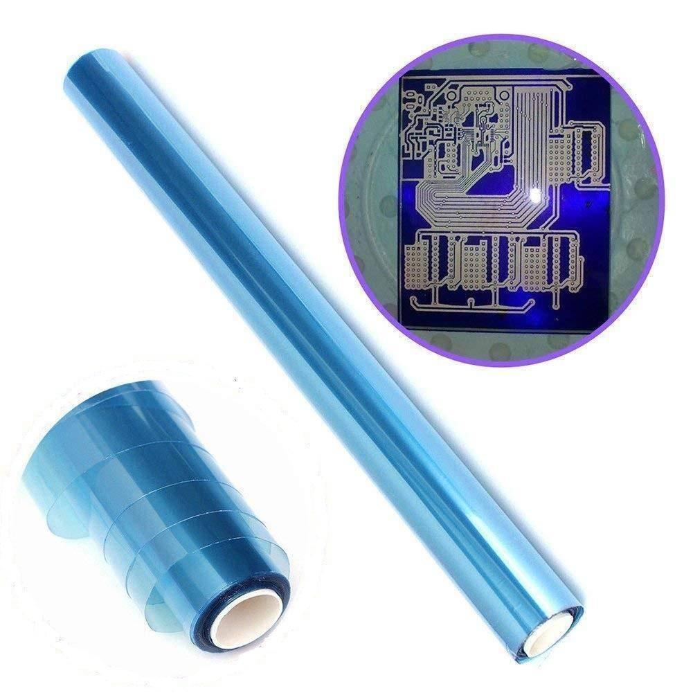


Discontinued Photo Resist Photosensitive Dry Film 30cm 1 Meter Photoresist
30cm Photosensitive Dry Film Replace Thermal Transfer PCB Board Length 1M. Photosensitive Dry Films. Photosensitive dry films are materials used in making the printed wiring boards of PCs, mobile devices, and other electronics. They are indispensable in the process of patterning the circuits of electronic devices. Process of Patterning Circuits of Printed Wiring Boards
Properties:
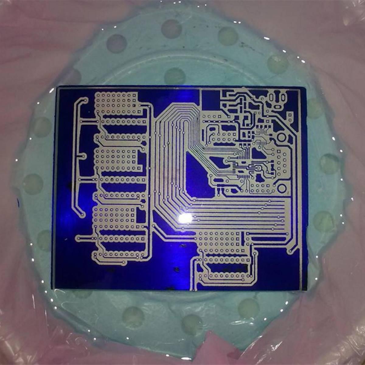
still, picture film, also known as the dry film used for making the PCB board, PCB top stick will have a sensing circuit.
- - Suitable for coating, hole covering etching process.
- - Excellent ability to cover the hole - High
Resolution
- Excellent adhesion to virtually all surfaces -
- image clarity exposure - Front panel is developed after the very clean
Feature:
- Width: 30cm
- Longth: 1M
- 1.5 mil thickness of dry film can be completely cover a hole of 0.25 inches
- The dry film can be used in the most ordinary plating solution, no wrinkle, no discoloration
- It can cut into 10pcs 15cm x 20cm film,and 5pcs 20cm x 30cm film. You can cut it as you like
Package Includes:
30cm width, 1-meter length Photo Resist Photosensitive Dry Film.
Operating steps:
- Grinding CCL, this simple, using the finest polished clean water frosted paper on the line.
- Removing film, photographic film is sandwiched between two layers of film, the first side can make use of transparent tape tear torn, try a few on the line.
- And then foil, copper clad laminates can look a little cleaner, pasted, try not to have bubbles.
- Good paste membrane used presses, not too hot, about 100 degrees from the fixing.
- The printed circuit board film, suggestion is to use film, the fine could reach the highest degree of accuracy if you did not ask for the paper to print it with sulfuric acid trip.
- The printed circuit on the photographic plate (Note: Dry film is negative, so to highlight the print, which we usually use photographic plate opposite) with ordinary energy-saving lamps 10 or so, if there is exposure Machine 1 minutes on the line, the sun not tried, it should be 30 seconds -60 seconds, the exposure process Obviously, since the photosensitive film will change color when exposed to light, the light becomes dark blue. You will easily see your circuit diagram appeared on the board.
- Developing and tear the protective film on the front panel, into the developer (developer according 1:100,10 g Total 1L of water) to be used when developing a little harder stick cotton wipe board.
- Etching, this goes without saying (ferric chloride etchant environmental protection, hydrochloric acid hydrogen peroxide, etc.) is recommended environmental etching shop, fast, clean, no odor.
- After a good CCL etching, stripping, from film watered by 1:60 or 70, the board bubble like a few minutes,
- After the completion of the board, very pretty good, most dense line spacing is 0.1MM, width 0.1MM, 0.1MM lines do know though is very easy to do, but do 0.1 lines and 0.1 line spacing dry film can easily do it.