Mosfet Igbt Driver Tlp250
Guaranteed Safe Checkout

Mosfet Igbt Driver Tlp250
Pin configuration isolated MOSFET driver TL250
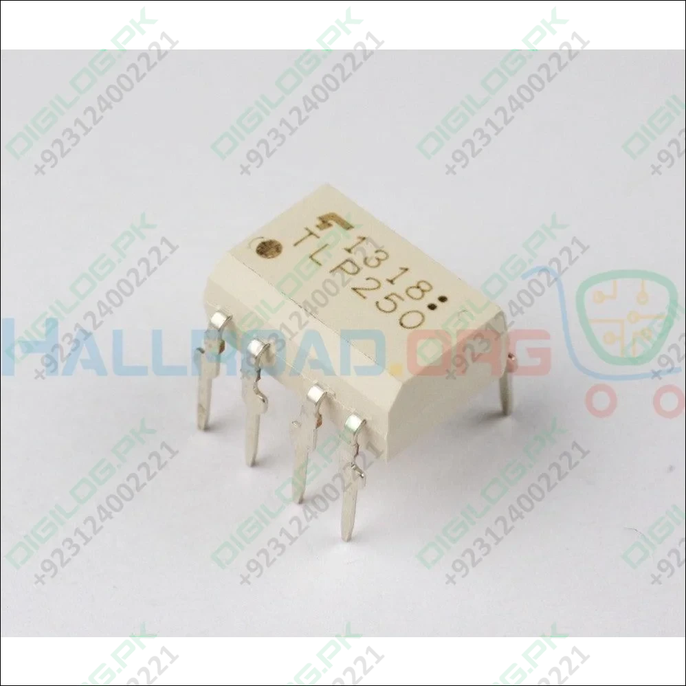
TLP250's pin layout is as follows. It is clearly shows in the figure that led at the input stage and photodetector diode at the output stage is use to provide isolation between input and output.
Firstly Pin number 1 and 4 are not connect to any point. Hence they are not in use. Pin 2 is an anode point of input stage light-emitting diode however pin 3 is the cathode point of the input stage. Input is provided to pin 2 and 3. Pin 8 is for supply connection. Pin 5 is for the ground of power supply.
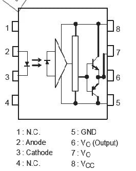 pin configuration of isolated MOSFET driver TLP250
Features:
- One and four are not physically connected to any point , so they are not in use.
- Pin 8 is used to provide power supply to TLP250 however pin 5 is the ground pin which provides a return path to power supply ground.TLP250 can receive a maximum power supply voltage of 15-30 volts dc, but this is also dependent on the environmental temperature for TLP250.
- Pin 2 and 3 are anode and cathode points of input stage LED. It works like a normal light-emitting diode. It has similar characteristics of forwarding voltage and inputs current because The maximum input current is in the range of 7-10mA and the forward voltage drop is about 0.8 volt. TLP250 provides output from low to high with a minimum threshold current of 1.2mA and above.
- Pin six and seven are connect to each other inside. Pin number 6 and 7 can be use to produce the output. Two transistors are used to configure a totem pole in TLP250. In case of high input, the output becomes high with output voltage equal to a supply voltage and in case of low input, the output becomes low with output voltage level equal to ground.
- Mosfet driver TLP250 can handle frequencies up to 250khz because of its slow propagation delay.
This all about pin configuration and working of TLP250. Now I will talk about how to used isolated MOSFET driver tlp250 as low side MOSFET driver and high side MOSFET driver.
TLP250 as a low side MOSFET driver:
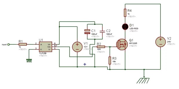
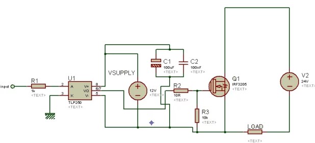
Circuit diagram of low side MOSFET driver using tlp250 is as follows. In this circuit diagram, tlp250 is uses as a non-inverting low side MOSFET driver. you should connect an electrolytic capacitor of value 0.47uf between the power supply. It provides protection to tlp250 by providing stabilize voltage to IC.
As shown in figure above input is drive signal that drives the output. Vin is according to signal ground. It should not be connect with supply ground and output ground. It is clearly shows in above figure TLP250 and load ground is refererence to the power ground and it is isolated from input signal reference ground.
When input is high, MOSFET Q1 get high signal from TLP250 and it is drive by power supply and current flows through the load. When input is low, MOSFET Q1 get low signal from TLP250 output pin and mosfet Q1 remains off and there is no current flow to load.
Value of supply voltage ranges between 10-15 volts. Usually input signal is provided through microcontroller and microcontroller input signal level is in the order of 5 volt. C1 decouples the circuit as the capacitor.
TLP250 as a high side MOSFET driver
Circuit diagram of MOSFT driver tlp250 used as high side driver is as follows. It is using as non inverting high side mosfet driver. Because input signal ground is connect to cathode of input stage light emitting diode. Therefore it is use as a non inverting high side mosfet driver.
In high side configuration there are three grounds as shown in figure above. Ground of input signal, ground of supply voltage and ground of power supply voltage. When using TLP250 as high side MOSFET driver, ensure that all grounds are isolate from one other.

