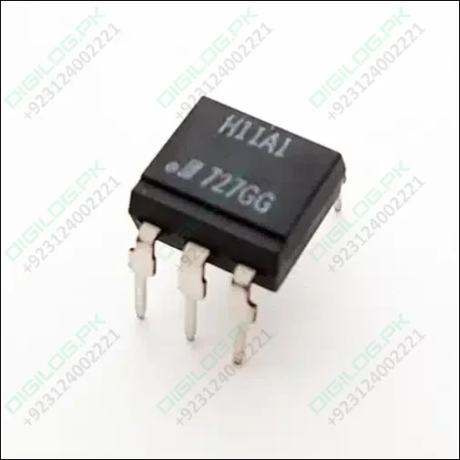
H11A1 Optocoupler DIP 6 Pin IC
Guaranteed Safe Checkout


H11A1 Optocoupler DIP 6 Pin IC
📘 H11A1 Optocoupler – Technical Data (DIP-6)
🔹 Description
The H11A1 is a phototransistor optocoupler.
It contains an infrared emitting diode (LED) and a silicon NPN phototransistor in a 6-pin DIP package.
It provides electrical isolation between the input and output.
🔹 Pin Configuration (DIP-6)
1 → Anode (LED +)
2 → Cathode (LED –)
3 → No Connection
4 → Emitter (Transistor –)
5 → Collector (Transistor +)
6 → Base (optional transistor base pin, usually left unconnected)
🔹 Absolute Maximum Ratings
-
Forward current (LED): 60 mA max
-
Reverse voltage (LED): 6 V
-
Collector-emitter voltage: 30 V max
-
Collector current: 50 mA max
-
Collector power dissipation: 150 mW max
-
Isolation voltage: 5300 VRMS
🔹 Electrical Characteristics (Typical Values)
-
Forward voltage of LED: 1.2V – 1.5V @ IF = 10 mA
-
Collector-emitter saturation voltage: 0.4V @ IC = 2 mA
-
Current Transfer Ratio (CTR): 50% to 600% (depending on binning)
-
Isolation resistance: >10¹¹ Ω
-
Coupling capacitance: <0.5 pF
-
Switching speed: 2 µs to 18 µs
🔹 Features
-
High dielectric isolation between input and output
-
TTL, CMOS, and logic compatible
-
Low coupling capacitance
-
Wide operating temperature range (–55°C to +100°C)
-
Base pin available for sensitivity adjustment
🔹 Applications
-
Logic signal isolation
-
Microcontroller I/O protection
-
Switch Mode Power Supply (SMPS) feedback
-
Telephone ring detection
-
Relay driver circuits
-
General purpose signal isolation
🔹 Typical Application Circuit
Input Side (LED drive):
Output Side (Phototransistor):
-
Base (Pin 6) → left open
-
When LED is ON → transistor conducts → output LOW
-
When LED is OFF → transistor cuts off → output HIGH
🔹 Internal Structure (Simplified)
-
Left side: Infrared LED
-
Right side: Phototransistor (NPN)
-
Separated by optical gap (no electrical contact, only light coupling)
Customer questions & answers
Ask a question
No questions yet. Be the first to ask!
