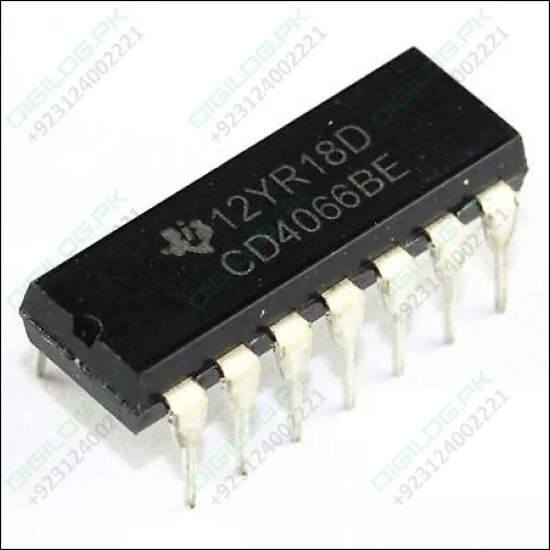
CD4066 Quad Bilateral Switch – Multiplexer
Guaranteed Safe Checkout

CD4066 Quad Bilateral Switch – Multiplexer

CD4066 Quad Bilateral Switch – Multiplexer
- Quad Bilateral Switch for Multiplexing
- Very Low Internal Resistance
- Operating Voltage: 3V to 18V
- Switching Voltage: 20V (maximum)
- On-state Resistance: 5Ω (at 15V Vcc and 10kΩ Load)
- Output current High: -0.4mA
- Low Level Control pin Voltage: 0.9V (max)
- High Level Control pin Voltage: 11V (min @ 15V Vcc)
- Available in 14-pin PDIP, GDIP, PDSO packages
The CD4066 is a Quad Bilateral Switch IC, that is, it has four switches which can be controlled individual using a control pin. These switches can conduct in both the directions making it bilateral, it is commonly used for multiplexing analog or digital signals. The switches have very low internal resistance making it suitable for audio applications.
Pin Configuration
| Pin Number | Pin Name | Description |
| 1, 3, 8, 11 | Switch Input A,B,C,D | Input pins for the four bilateral switches |
| 2, 4, 9, 10 | Switch Output A,B,C,D | Output pins for the four bilateral switches |
| 5, 6, 12, 13 | Control A,B,C,D | Control pins for the four bilateral switches |
| 7 | Ground | Ground pin of the IC |
| 14 | Vcc | Pin to power the IC |
Customer questions & answers
Have a question? Get answers from customers who have purchased this product.
Ask a question
No questions yet. Be the first to ask!
